Discovering the Panasonic JR-200U
I had never even seen a Panasonic JR-200U before 2012, but when I did, I became curious. What kind of secrets does this oddball 8-bit contain? This page is a collection of several useful bits and pieces I’ve come across so far. Corrections and additions are most welcome. Some of the findings are correct only for the PAL JR-200UP model, since that’s the only one I have at my disposal. Big thanks to Tero Heikkinen for his contributions!
Pretty much all the information you see on this page is based on disassembling the ROM, individual chips’ data sheets, and simply trying things out. Jeff from Vintage Volts was so helpful as to scan the US version of the Service Manual, which helped to clarify some issues. Grab it here. As there’s better info available now, I’ve removed some inaccurate paragraphs from this page altogether. Do note that there are some differences between the NTSC and the PAL versions, esp. in clock pulse generation and rates, so even the Service Manual isn’t always authoritative.
CPU
The main processor is an MN1800A, a clone of the Motorola MC6802 (which itself is a revision of the MC6800). The most notable difference is that the MN1800A does not have an internal oscillator. The A version of the chip can cope with speeds up to 1.5 MHz, whereas the normal one is limited to 1 MHz. Not much to see here:
- Two 8-bit accumulators, A and B
- 16-bit index register, X (IX)
- 16-bit stack pointer, S (SP)
- 16-bit program counter, PC
- Condition code register, CCR
The MC6800 features quite many addressing modes. Among the most interesting ones is the direct mode, which lets you access the first 256 bytes (the zero page) of the RAM quickly. Most of that area is occupied by system and BASIC variables by default.
I’m still trying to solve the actual clock speed of the CPU, as that 0.89 MHz has just been mindlessly repeated here and there. As the display controller divides the NTSC-derived xtal 14.31818 MHz frequency with some probably 2n counter, it’d be natural that the CPU gets something related to that. Indeed, dividing the standard NTSC carrier frequency by four yields 0.894886 MHz.
However, that is not the processor speed. My current guess, based on code run in VRAM, is 1.366 MHz. On the other hand, the frequency doesn’t quite reveal all there is to it, as the speed is normally constrained by the 1-bit DRAM access. As fetching is exceptionally slow, instructions suffer from various penalties, for example:
- Nop is 2 cycles on paper, but in practice 4 – you can’t do anything in less than four
- Some one-byte instructions like tsx jump from 4 to 6 cycles
- But an ldaa offset,x takes full 8 cycles instead of 5
- Even worse, an ldaa address (extended) crawls at 8 cycles, not its nominal 4
- A 7-cycle inc offset,x takes 11
- An ldx address is one of the worst performers, 5->10
Go figure. I’m trying to gain a better understanding of the timings, but as of now it seems kind of random. One of the most exceptional things is that VRAM is 2x as fast as normal memory – kinda logical, though, as it’s 8-bit SRAM unlike the other chips (see below). In practice this means that the most timing critical parts should definitely be stored in VRAM, where instruction timings also match the nominal cycles.
System chips
The following chips can be found on the circuit board:
- 6914 — dual comparator, used for tape communication
- HD7416P — hex inverter/driver, amplifies the video signal
- HD61L204F, surface mounted. HD61K201F on the NTSC model.
- The display controller (CRTC)
- Divides clock signals (phi1 and 2) for the CPU and phi2S for the MN1271
- Address decoder
- Probably some other yet unknown functions
- HM4864P-3 — 8k dynamic 1-bit RAM, four chips make 32k altogether
- HM6116P-3 — 2k static RAM, two of these constitute the 4k VRAM
- MN1271 — I/O interface, includes the clock and beepers
- MN1544CJR — 4-bit microprocessor
- Used for keyboard and joystick I/O
- Contains 4k of ROM including the system charset, and 128 bytes of RAM.
- MN1800A — the CPU
- MN4864CA2 and CB2 — 8k rom chips
- Several 74LS series logic chips:
- 74ALS112AN — flip-flop
- 74LS00 — AND gate
- 74LS04 — inverter
- 74LS05 — inverter
- 74LS08 — AND gate
- 74LS145 — BCD decoder, between the keyboard and MN1544CJR
- 74LS245 — octal bus transceiver, on the data bus
- 74LS367A — 3-state buffer
- 74S163N — 4-bit counter
- M74LS00P — NAND gate
Another important part is the 44.336 MHz xtal (X1) under the modulator. On an NTSC machine the same oscillator is 14.31818, so the timings are generated differently. Tero took some high resolution photos of the guts an put them online. Check out the images here.
Graphics
The JR-200 has only one screen resolution, 256×192 pixels with eight colors, but bit 7 of the character color lets you select an additional blocky low-resolution mode for each character position. There’s two kilos of VRAM plus two more for the character bitmaps. Unfortunately, there’s not enough space for two full pages. The text resolution is 32×24 (768 positions) and the bitmap for each 8×8-pixel character can be redefined. The border color can be set separately. Eight colors are available in a typical three-bit GRB format:
- 0 — black
- 1 — blue
- 2 — red
- 3 — magenta
- 4 — green
- 5 — cyan
- 6 — yellow
- 7 — white (guess what)
Bits 0–2 of the color table define the fg color of the respective character position, and bits 3–5 the bg color. Bit 6 selects the charset base address, and bit 7 switches the character position in question to lowres mode, where a 8×8 pixel region is split into four 4×4 blocks, effectively yielding a 64×48 resolution where each pixel can be set individually. The upper half gets its colors from the character position table, and the other half from the color table. When bit 6 is zero, the character bitmaps are read from $D000. Value 1 sets the base address to $C000, which is rather inconvenient, since it overlaps with the character positions and colormap, except at two locations: $C000–$C0FF and $C400–$C4FF. Thus, characters 0–31 and 128–159 can be relocated without overlaps, yielding 320 different possible characters (256+32+32).
So far it’s unknown whether there’s any exact way to sync to the screen refresh. There’s no VBI, and judging by the existing games, there’s no way to read the refresh phase easily. Luckily, the timer can be reprogrammed to serve as a VBI. For an exact 50 Hz PAL sync the values are 3414 for three frames and then 3413 for one. Screen refresh can be — to a certain extent — followed by reading the memory addresses starting from $CA00, which return the last attribute shown on the screen or just some bus traffic in the borders. The timing is a bit tricky, but by drawing a suitable pattern and setting the clock according to that it’s possible to create a usable VBI.
This shiny new routine takes a while to calibrate but is about two row exact: vbinew2.s. The calibration might fail under some rare conditions, when other unrelated bus values happen to match the needed colors. Couldn’t break it with 30 consecutive test runs, but I’ve seen it happen. For the sake of completeness, here’s the old coarse and less reliable version that starts quicker: vbi.s.
Another, more robust solution would require a minimal hardware mod involving a piece of wire that connects the VSYNC signal to for example the user interrupt or just some pin of the printer/expansion port. So far I haven’t tried that, as the software method works well enough on a PAL machine at least.
The graphical capabilities of the Spectrum computers aren’t that far from the Panasonic and there are truckloads of great pictures available, so I wrote a little converter in Processing to turn 256×192 images into something you can display on the JR-200. This directory contains some converted images — apologies if your hard work was ruined in the process 🙂 320 blocks aren’t usually enough to reproduce the original exactly. Run them like this:
mload:a=usr($1000)
Sound and timers
According to Wikipedia and Old-Computers.com there should be three separate square wave channels capable of five octaves. JR-100, on the other hand, only had a simple one-channel beeper. MESS source code implies that JR-200 might contain a good old PSG, AY-3-8910, but on the circuit board there’s no such thing to be found. Some experimenting and ROM disassembly finally revealed the sad state of affairs: there is no sound chip. Instead, it’s the clock and I/O chip, MN1271, that produces the beeps.
MN1271 contains two 16-bit timers (E and F) plus four 8-bit counters (A–D):
- A controls serial communications speed
- B is the obscure “bpm timer” (can’t really figure out much use for this)
- E is used as the system clock and generates an IRQ every 0.1 seconds by default
- C, D and F are connected to the speaker and used for square wave generation
That’s three sound channels, but C and D can only produce a narrow range of different frequencies, being 8-bit. No noise, volume settings, envelopes or filters, just three square waves out of which two are very limited. With low frequencies the output starts to look more like saw wave, since the level fades towards zero.
Each timer has a control byte and an 8-bit or 16-bit counter. The three lowest control bits must contain 6 in order to keep the timer running. Any other value will stop the timer (just speculating here that there are probably some unknown pulse counter and edge triggered modes). The higher bits define other important parameters (see below). Under normal conditions the control byte of E contains $4E. The beeper timers’ control byte depends on the octave that is being played back or zero if the channel is off. All the timers can generate an IRQ, so in that sense E is not special at all. Known control bits so far:
- 7 — not used (?)
- 6 — interrupt on counter zero if 1
- 5 — not used (?)
- 4..3 — divisor selection. 00 = 1, 01 = 8, 10 = 64, 11 = 256. They correspond to OR values 0,$8,$10 and $18 .
- 2..0 — Timer runs if 110 (6), stops otherwise
To reprogram the timer speed all that is needed is a new counter value. My best guess on the base frequency at the moment is 1.366 MHz, which you divide by the desired divisor and frequency to get the counter value. According to the Service Manual the frequency is 1.34 MHz for an NTSC machine, but as the timings seem to be quite cursory in it anyway, I wouldn’t trust that number much. Note that 1 is the smallest possible value, since 0 is considered to be 256. For 16-bit counters poke the hi byte and then the lo byte to their respective addresses. See the memory map below for the memory locations of each timer. For square waves you need to divide by 2*frequency, since a full wave requires two changes. Here’s a list of the closest 16-bit counter values for notes using divisor 8: jr200notes.txt (might be revised later).
Since there were apparently no existing tools for creating music I spent one weekend writing a little music converter and a player routine that let you convert XM tunes to Panasonic beeps. The composer needs to be aware of the harsh limitations imposed both by the simple routine and the less-than-stellar sound chip, but at least this is a bit easier than typing hex into assembler data statements. Without further ado, go ahead and download Musagi.
Keyboard and joysticks
The keyboard and joysticks are connected to the MN1544, which checks their status and interrupts the main CPU when there’s activity. Normally the system doesn’t read the joysticks at all, just the keyboard (see memory map below for the locations of the related buffers). The last keypress can be read from $C801, but it’s not enough for games, since you can’t tell whether the key is still pressed or not. Even the BASIC interpreter features a function called STICK, which lets you read the keyboard and joysticks as directly as possible. From assembly the same subroutine can be called at $E8CB (slowjoy.s). It’s still impossible to read whether a particular key is pressed or not, but at least the joysticks work perfectly.
The biggest problem with the approach is that it takes about 1/4th of a frame to complete the call, since the subroutine needs to wait for three interrupts coming from the 1544. Communication with the 1544 is kind of hairy business, but luckily the joysticks can be read fast by first setting the correct mode, doing something useful while the three interrupts take place, and reading the result only then (fastjoy.s).
It’s still unknown whether the current status of an individual key can be read at all. Probably not, and even if yes, it would be unusably slow with all the interrupts involved. The keyboard matrix and operation are explained in some detail in the Service Manual, pages 52–55.
It turns out that the joystick ports are identical to those of the MSX: there’s +5V and strobe on the same pins. What that could mean is that an MSX mouse could theoretically work on the Pana, depending on the implementation of the MN1544 keyboard reading code. I’m a bit skeptical, though, as the standard joyport functions are so slow, plus they might not let you control the strobe pin correctly.
Expansion bus
The mapping of the expansion port pins can be found on page 62 of the Service Manual. Some random notes:
- Signals such as vma, r/w and phi2 are inverted along the way, so they follow a different logic than the CPU
- Phi2s is meant for dividing memory access between the CPU and the video controller. If you output at the wrong moment the screen will flicker.
- The !kill signal disables the BASIC ROM at $A000..$BFFF
- Data pins are buffered through IC3
- Pins A19 and B19 are +5V, but don’t seem to be able to supply a lot of current. Better consider an external PSU for your extensions.
The printer port or the CNIO header found near the TV modulator would be other easy options for moving data about, as they are directly connected to parallel ports of the MN1271. See the memory map below. However, they won’t allow for an autobooting ROM, unlike the expansion port.
Memory map
First a general view (click to see full size). A similar chart is available on the Operation Instructions, page 51 and the Service Manual page 20.
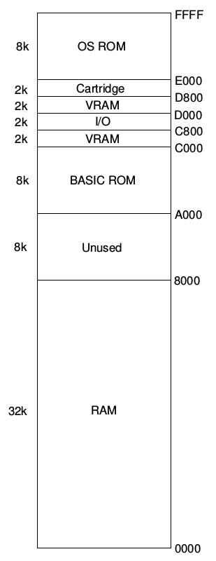
Know addresses in more detail:
- $0000–$7FFF: 32k RAM
- $0000: key click (0 off, $40 on)
- $0001, $0002, $0003: direct keyboard and joystick call data area
- $0004: 8-bit 0.1 second down counter
- $0005: 8-bit 0.1 second down counter running from 10 to 1
- $0006: 16-bit one second down counter
- $000D: unhandled keypress counter, used for other communication with 1544 too
- $002B: tape load speed (0 = 2400 bps, 1 = 600 bps)
- $002C: tempo, 109 by default
- $002D, $002E, $002F: PLAY note duration counters
- $0030, $0032, $0034: PLAY note buffer pointers
- $0036, $0039: tempo counters
- User-provided interrupt handler addresses. $0000 if not used.
- $0100: NMI
- $0102: sw interrupt
- $0104: IRQ
- User hook addresses
- $0106: unknown hook
- $0108: unknown hook
- $010A: unknown hook
- $010C: timer hook, runs every 0.1 seconds
- $010E: one second timer hook
- $0114: transfer buffer from 1544 (?)
- $0116: 16-bit keyboard buffer pointer
- $0150: keyboard circular buffer of 32 bytes, alternatively keyboard data for STICK(0)
- $0151: joystick data for STICK(1)
- $0152: joystick data for STICK(2)
- $07FF: default stack
- $0800: start address of BASIC programs
- $8000–$9FFF: not used
- $A000–$BFFF: 8k BASIC ROM
- Video RAM
- $C000–$C7FF: alternative character bitmap (overlaps with other tables)
- $C100–$C3FF: character positions
- $C500–$C7FF: character colors
- $D000–$D7FF: character bitmaps
- $C800–$CFFF: Memory-mapped I/O
- MN1271 I/O interface
- $C800: parallel port A control, normally 0
- $C801: parallel port A data, used for keyboard reading. The code is already ASCII.
- $C802: parallel port B control. Bit 0 enables the keyboard interrupt.
- $C803: parallel port B data, used for issuing commands to the MN1544 and for misc purposes. Bit 6 controls the keyboard beep.
- $C804: parallel port C control
- $C805: parallel port C data, the printer port
- $C806: parallel port D control, used for tape communication
- $C807: parallel port D data. Bit 6 controls tape relay (write). Loud enough negative sound signal turns bit 7 on (read). The rest go to the CNIO header.
- $C808/9: parallel port I control/data — unconfirmed
- $C80A: used for keyboard ACK, read after the keyboard port
- $C80B/C/D: unknown, most likely serial stull
- Timers (part of the MN1271)
- $C80E: timer A control (serial timing) — unconfirmed
- $C80F: timer A counter, 8-bit — unconfirmed
- $C810: tempo timer (B) control, contains $59. Doesn’t work quite like the other timers.
- $C811: tempo timer (B) counter, in bpm
- $C812: timer C (beeper) control
- $C813: timer C counter, 8-bit
- $C814: timer D (beeper) control
- $C815: timer D counter, 8-bit
- $C816: timer E (system clock) control
- $C817: timer E counter hi, default $41
- $C818: timer E counter lo, default $8A
- $C819: timer F (beeper) control
- $C81A: timer F counter hi
- $C81B: timer F counter lo
- Interrupt control (part of the MN1271)
- $C81C: interrupt status register 1 (read). Bit 0 = keyboard.
- $C81D: interrupt status register 2 (read). Bit 4 = timer, bit 1 = tempo timer.
- $C81E: interrupt mask register 1. Bits as above, default value 1.
- $C81F: interrupt mask register 2. Bits as above, default value $12.
- I/O area wraps to the beginning every 32 bytes until $C9FF
- $CA00: border color — in fact any address up to $CBFF works the same
- When read, the addresses starting from $CA00 return the last attribute displayed on the screen and some unknown values while in the border area (just the bus traffic?).
- MN1271 I/O interface
- $D800–$DFFF: cartridge region
- If there’s a long jump (opcode $7E) at $D800, then the OS ROM jumps there after initializing the system. If not, it jumps to BASIC at $A000.
- $E000–$FFFF: 8k OS ROM
- Interrupt handlers
- $E6E4: reset handler
- $E790: NMI handler
- $E7DC: software interrupt handler
- $E7E2: IRQ handler
- $E892: idle loop
- $E8CB: direct keyboard and joystick call. Return values stored at $0001, $0002 and $0003.
- $FED8: error messages
- $FFA4: startup text
- 16-bit interrupt vectors
- $FFF8: IRQ
- $FFFA: software interrupt
- $FFFC: NMI, triggered when break is pressed
- $FFFE: reset vector
- Note that the vectors are in ROM and, therefore, can’t be directly changed. Use the optional handlers and hooks starting from $0100.
- Interrupt handlers
Still missing quite a lot of relevant stuff and details.
File transfer and creation
I don’t know if the floppy drive was ever sold outside of Japan. “Disk BASIC” is mentioned on the Service Manual, but even so practically nobody owns it, so we’re stuck with cassettes. A very typical approach these days is to emulate a tape drive by playing back sound files from a modern host computer to the cassette port. For an in-depth description of the tape format and the associated CJR emulator files check the Old Machinery blog (see below). Credits go to Tero Heikkinen for documenting the format. My tools for dealing with CJR files:
- bin2cjr.c — converts binary files to CJR
- cjr2wav.c — converts CJRs to audio files that can be played back to the cassette port. Seems to work with 2400 bps files only.
- cjrinfo.c — displays all relevant info such as the file type, block numbers, lengths and addresses
When loading your own programs do something like this on the Pana:
mload:a=usr($1000)
Raw wav files tend to be a bit on the big side — a tiny 7k CJR turns into a 2 MB wav with the above converter. Gzipping the wav makes it way smaller, just 55k. Lossy formats, such as mp3, might distort the waveform too much, but at least 128kbit files seemed to work just fine. The file size decreased to 763k, but the resulting mp3 can’t be effectively compressed any longer. YMMV.
Here’s my LZSS compressor and a 6800 machine language decompressor routine for your enjoyment. Together they constitute PanaZ, a simple exe packer that can be used with your plain binary files before turning them into CJRs. See the zip file for further instructions.
Panana 1.0
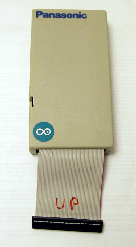
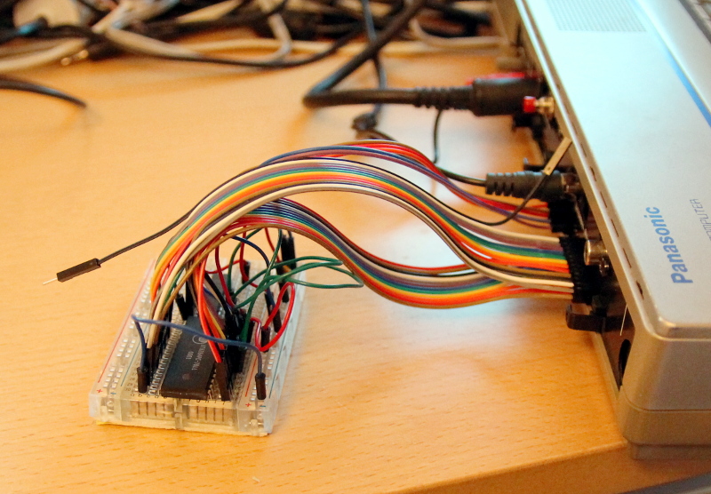
As there are no realistic emulators available as of now, it’d be mandatory to easily test own programs on a real machine. Beeping the program in through the cassette port gets you started but, honestly, it’s too slow: it takes around a minute and a half to transfer a binary file of a mere 20 kilobytes. Moreover, you need to type the loading commands all the time. To overcome those irritating limitations, I developed an Arduino-based “coder’s cable” with and autobooting ROM that contains the transfer slave. First, here’s some work-in-progress shots for your enjoyment:
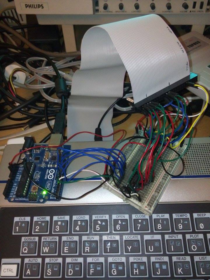
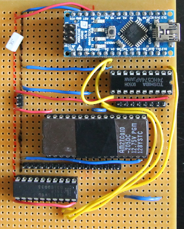
The circuit board in the middle isn’t the final version, so don’t use it as a reference. With the latest improvements I’ve reached transfer speeds up to 8k/s – a whopping 30x speed increase compared to the cassette port. In other words, you can fill the memory up in four seconds. After some final improvements Panana seems to be stable even with a trashy Chinese Arduino Nano clone. There are still several shortcomings, such as the lack of support for multipart or BASIC CJR files (needed for games), but as those are not needed for software development, I’ve had little interest in implementing them at least as of now. Another detail I’m not awfully happy about is the huge 128k EPROM chip that takes a lot of space and is almost empty. Got them really cheap, you see.
And then the schematics. Note that !reset is only needed with a Leonardo or a Micro, as they don’t reset automatically when receiving serial input. On the other hand, it very much improved reliability with the trashy Chinese Nano clone that I used.
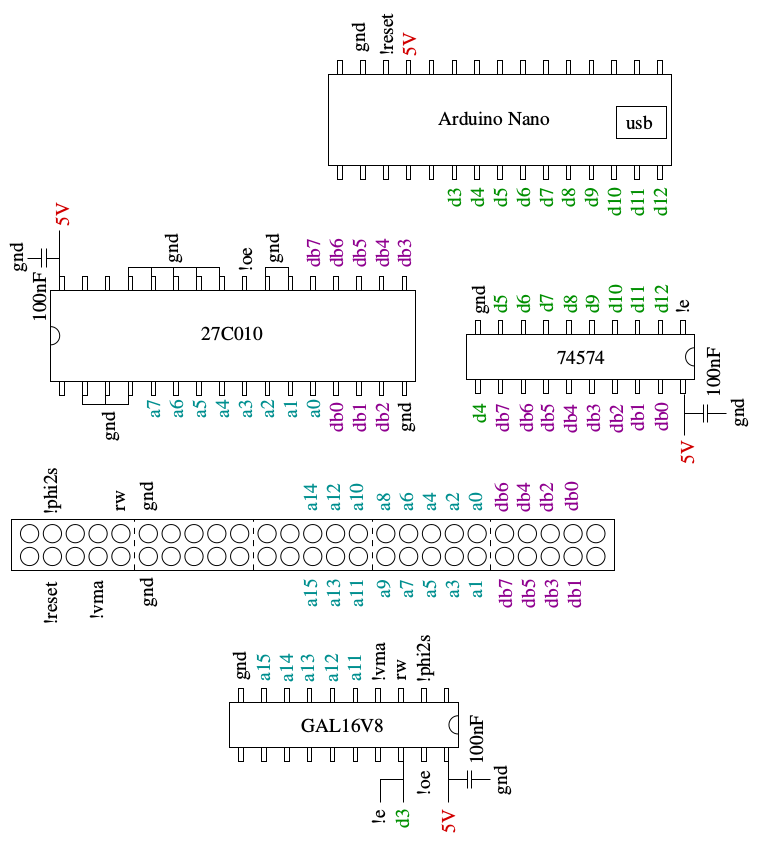
Download the required software here: panana-1.0.zip. Inside the zip you will encounter:
- host – File transfer software C sources. Meant for Unix-like systems with termios, such as Linux or Mac OS X. For other platforms you need to modify the parts that access the serial port.
- jr200 – The ROM for the JR-200. The source can be compiled with CRASM.
- arduino – The sketch that needs to be uploaded to the Arduino. Tested with an Uno and a Nano clone, but should work fine on other similar boards. Leonardo and Micro will need a reset wire (see above) as they don’t reset themselves when receiving serial traffic. Duemilanove should be fine as is.
- gal – The equation for the GAL in .eqn format. Can be recompiled to .jed with eqn2jed.
As you can see, this is no turn-key solution, so you may experience hiccups and, all in all, need to have a positive and proactive attitude to get anywhere with it 🙂 It’d be awesome to turn Panana into a real PCB one day, but let’s see if I ever get that far.
When you boot the JR-200 with the Panana and a USB cable connected, you should see letter P in the top right corner. The file transfer host controls whether the CJR will be started automatically or not. If not, after the transfer the machine will jump automatically to BASIC. Other characters you might see are E for error or a heart denoting a succesfully completed operation.
8k SRAM memory expansion
Something evident on the memory map is that it should be rather straightforward to extend the memory to 40k through the expansion port. Even 48k could be possible, since you can disable the BASIC ROM through the port. I gave it a go one beautiful Saturday and indeed, it is easy to add that 8k by wiring the address and data lines plus some more from the expansion port to a SRAM chip. Three highest bits of the address need to be decoded, too, which is a good job for a GAL.
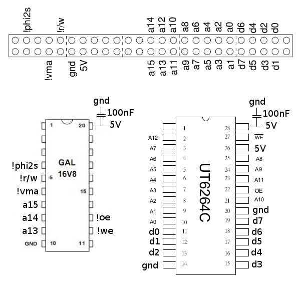
A bit lousy schematic it is, but at least it works. Here’s the function needed for the GAL16V8. Compile to .jed with the usual eqn2jed.
CHIP GALLI 16V8

i0=1 i1=2 i2=3 phi2s=4 rw=5 vma=6 a15=7 a14=8 a13=9 gnd=10
i3=11 we=12 oe=13 o0=14 o1=15 o2=16 o3=17 o4=18 o5=19 vcc=20

EQUATIONS

/we = a15 * !a14 * !a13 * !vma * rw * !phi2s
/oe = a15 * !a14 * !a13 * !vma * !rw * !phi2s
The BASIC doesn’t recognize the extra 8k, but you can mload and run code there without problems. Even a timing critical IRQ handler worked just fine. The prototype could be extended to 16k with an optional BASIC on/off switch, or even to several megabytes by introducing a banking scheme of some sort. As my target is the standard machine, such an extension isn’t a priority.
Reset button
A memory-preserving reset button can be useful for a developer, cracker or a cheating gamer, too. Based on p. 29 of the Service Manual it was easy to make a – hopefully – safe reset button. You could ground the processor /HALT pin directly, but this one is safer, as the signal goes through two inverters and there’s a capacitor to filter the noise caused by lousy buttons (like mine). See here:
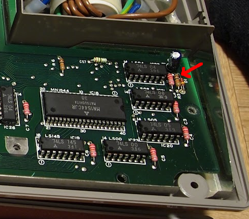
First find the capacitor and diode (D1) at the top right corner of the mobo. Solder a wire to the back leg of the diode, add a button and connect the other leg of the button to the ground. For example the screws holding the mobo in place are grounded, so you can wrap the wire under one of them.
Software
There’s not much to talk about, I’m afraid 🙂 I’ll update this section when I’ve taken a closer look at the games that came with the Virtual Panasonic emulator. Here’s some PAL/200UP stuff by my group Fit:
- Panyansonic, a little demo with a feline theme. A video for those who don’t own the real deal.
- SR-200, probably the first ever program to feature smooth scrolling. Plus an ugly YouTube video capture.
- See also the directory of converted Spectrum pics.
Run with mload:a=usr($1000). Any contributions would be most welcome; just sample the cassette contents and send the files to me. Those rare Disney games would be an interesting find.
Sources
- Old Machinery’s entry on JR-200U (another Finnish page – we’re living in a Panasonic nation)
- Further description of the CJR format
- Tape audio format description
- MESS source code, a somewhat useful resource even with its shortcomings
- Virtual Panasonic JR-200U. The best emulator for the JR-200. An easy introduction to JR-200, but don’t expect too much if you’re after hardware tricks and exact timings. Windows-only, although runs quite ok with Wine.
- Disassembled versions of the basic and system ROMs. Not sure about their correctness, but in theory it’s all in there.
- Old-Computers.com’s entry on the ancestor, National JR-100
- Interesting scanned ads and manual pages by Gust Notch
- CRASM, one of the many cross-assemblers that can deal with the 6800. My example sources are for CRASM.
- The Service Manual provided by Vintage Volts.
- Various developer documentation provided by Lance F. Squire.
- Motorola 6800 microprocessor architecture
- MC6802 datasheet, full of useful information such as the execution times
- Motorola 6800 Instruction Set Summary — a quick reference
- MC6800 Application Manual
- My source code directory. Everything is under public domain, so use as you see fit.